
Negeri Sembilan unveils a US$20 billion photonic AI manufacturing hub, creating 60,000 jobs and positioning Malaysia as a leader in next-generation semiconductors.
SEREMBAN: Negeri Sembilan has announced the development of the Nilai Advanced Photonic AI Manufacturing City, the first large-scale photonic computing and semiconductor initiative of its kind in the world.
The project is being realised through a collaboration between the Hosein Family Office (USA) and the Gan Family Office (Malaysia).
Mehamood Hosein, founder of deep-tech Hosein Family Office, is leading the initiative with more than 30 years of global experience.
The Gan Family Office is contributing 1,214.06 hectares (3,000 acres) of land.
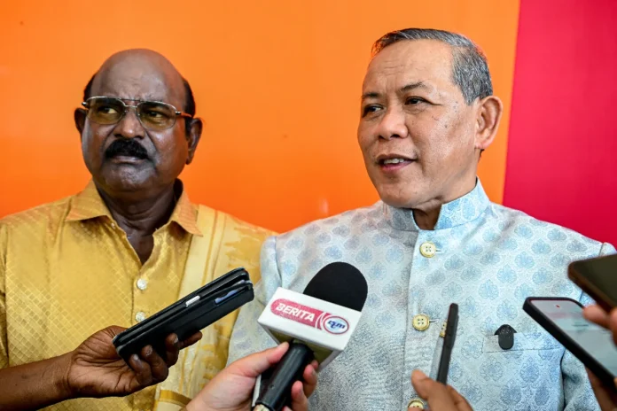
Menteri Besar Datuk Seri Aminuddin Harun said the project is planned at a scale of about US$20 billion over the next five years.
“This includes 40,000 high-paying skilled jobs, 20,000 indirect jobs across supporting industries and a total of 60,000 long-term employment opportunities,” Aminuddin said.
He said the development will include photonic chipset integration facilities, glass interposer and waveguide factories, and AI compute system assembly lines.
It will also feature a national real-time AI and digital twin research centre, a deep-tech training academy, and an integrated township.
Aminuddin said the city will introduce breakthrough photonic computing, where data moves through light instead of electricity.
“This enables dramatically higher speeds, lower heat, and far greater energy efficiency, allowing Malaysia to leapfrog traditional electrical semiconductor manufacturing,” he said.
He said photonic architecture is widely regarded as the next platform for semiconductor technology.
This positions Malaysia among the first nations to build the semiconductor platform of the future and the first large-scale photonic semiconductor manufacturing hubs in Southeast Asia.